PCB
Our customers come from various sectors, specializing in satellite phones, cell phones and portable smart devices. We also engineer products for heavy industry, including testers for circuit boards and products, and high voltage and ATEX class circuit boards.
Offering Overview
A Printed Circuit Board (PCB) serves as the backbone of most electronic devices. It’s a flat board that connects all the electronic components in the device, such as capacitors, resistors, and microchips.
PCBs are designed to be compact and efficient, fitting into various devices from small gadgets like antenna tags to larger appliances like mobile/satellite phones. They are made through a process that involves printing, hence the name "printed" circuit board, where the layout of electrical connections is first designed and then printed onto a non-conductive material, typically a type of hard plastic.
Where is this offering applied?
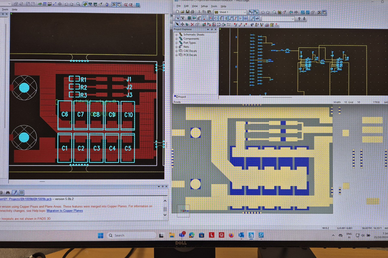
Sasken’s PCB layout department offers expertise in circuit board design, evaluation, and utilization of diverse design tools. Collaboration between different departments, including mechanics, RF, audio design, and BB, is seamless. The team has ability to convert files from certain PCB design software to compatible platforms like PADS, PADS Pro, and Zuken.
The PCB layout department offers circuit board design to the customer from start to finish, including circuit diagram design, component creation, layout, generation of manufacturing documents, and ongoing support throughout manufacturing processes.
Addressing customer needs
The customers' challenges often include a lack of software, employees, or time, or they may lack expertise in circuit board design. Sasken addresses these challenges with flexible cooperation, helping to meet strict design limits and resolve issues before final production and delivery. Sasken offers tailored expertise or integrated solutions across departments. Our PCB layout department excels in designing from simple to complex multi-layer boards and provides inspections, improvements, and troubleshooting for various circuit board issues.
A closer look at Sasken offerings
The PCB layout department has expertise across multiple circuit board software platforms, such as PADS, PADS Pro, and Zuken CR-8000. Our expertise spans various areas including circuit diagram design, library component creation, circuit board layout, component parts list generation, structural design of circuit boards, documentation, manufacturing instructions for both circuit board manufacturers and assembly processes, 2D and 3D translations for mechanical purposes, as well as collaborative knowledge sharing with other departments concerning circuit board-related matters.
Tools and technologies utilized
In the PCB layout department, we utilize a range of tools such as Mentor PADS, PADS Pro, and Zuken CR-8000. We can also convert Mentor Expedition files to the PADS Pro tool. Our toolkit includes CAM350 software for PCB manufacturing file viewing, along with mechanical tools like Catia and Inventor to facilitate the integration of circuit board designs with mechanics.

CASE STUDY

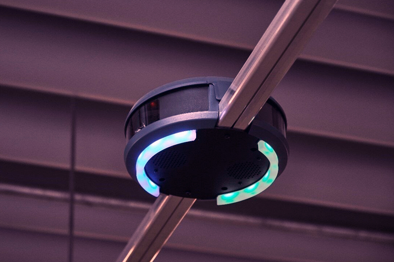
Automatic ceiling mounted guidance system
Read More →
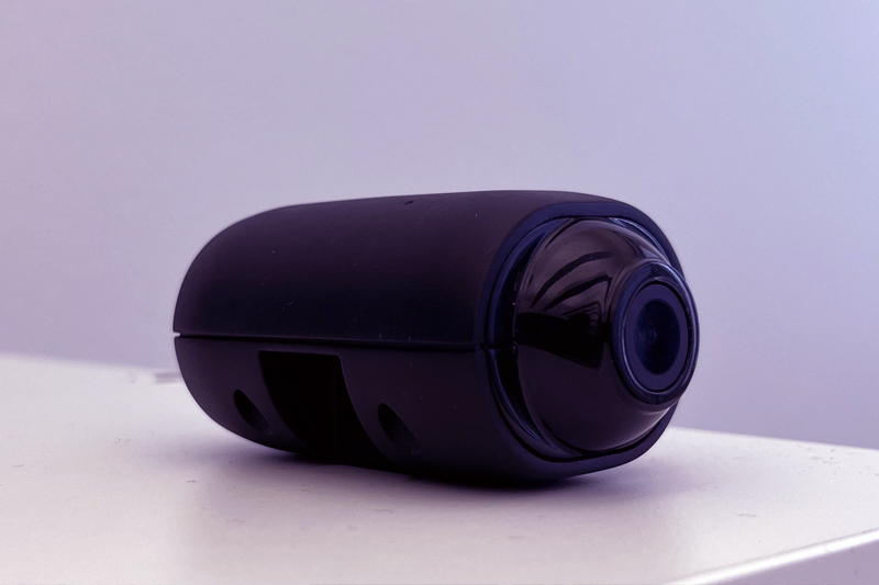
Driver assisting multi-camera system
Read More →
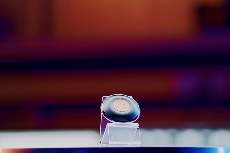
Bluetooth Smart TAG
Read More →
