

Competence Offering
PCB
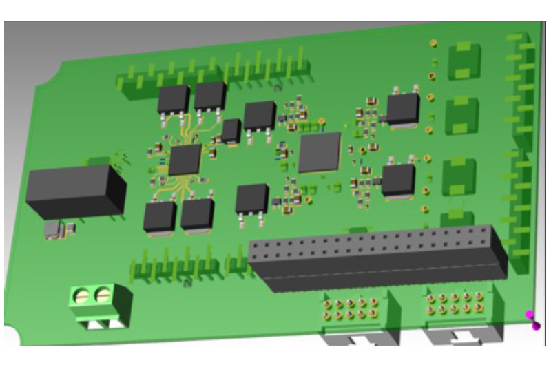
Sasken delivers more than PCB layout services. We provide end-to-end PCB engineering covering architecture support, schematic design, high-speed layout, signal integrity analysis, prototype validation, and production support.
Overview
Why choose Sasken for PCB design?
Sasken delivers more than PCB layout services. We provide end-to-end PCB engineering covering architecture support, schematic design, high-speed layout, signal integrity analysis, prototype validation, and production support.
Our experience spans industrial, communication, satellite, automotive, IoT, and embedded systems where PCB performance directly impacts overall product reliability and functionality.
Key added value comes from:
- Faster development through simulation-driven design and early verification
- Optimized signal integrity and power distribution for complex systems
- Reduced manufacturing risk through DFM, DFT, and production-focused design
- Expertise in high-density, multilayer, and high-speed PCB technologies
- Seamless integration with RF, antenna, mechanics, and embedded software
- Support from concept development to mass production
By combining electronics expertise with system-level understanding, Sasken helps customers develop robust and manufacturable products while reducing redesign cycles and time-to-market.
Core Expertise
Core expertise
Our PCB engineering capabilities cover the entire development process, from schematic capture and architecture support to high-speed layout and product validation. We work closely with electronics, RF, antenna, mechanical, and software teams to ensure the PCB supports overall system performance.
Core competencies include:
- Schematic design and PCB layout
- High-density and multilayer PCB design
- Signal integrity and power integrity analysis
- High-speed digital design
- RF and mixed-signal PCB design
- Embedded and industrial electronics
- Thermal-aware PCB design
- Design for manufacturing and testing (DFM/DFT)
Our team has extensive experience in communication devices, satellite terminals, industrial automation, smart grid solutions, camera systems, and IoT products.
Optimization
Performance and optimization
Modern electronics require PCB designs that deliver reliable performance while meeting demanding size, cost, and manufacturing requirements. Sasken utilizes simulation, analysis, and validation methodologies to optimize designs before production.
How we create value:
- Signal integrity analysis for high-speed interfaces
- Power integrity optimization and power distribution design
- EMC and EMI risk mitigation
- Thermal analysis and heat management
- Component placement optimization
- Stack-up definition and routing strategy development
Through early verification and close collaboration across engineering domains, we help prevent costly redesigns and ensure stable product performance throughout the development lifecycle.
Deep Dive
Advanced capabilities
Sasken supports demanding PCB projects where complexity, reliability, and performance are critical success factors. Our engineers have extensive experience designing products operating in harsh environments, complex RF systems, and mission-critical communication applications.
Specialized capabilities include:
- High-density interconnect (HDI) PCB design
- Multilayer high-speed architectures
- Satellite and wireless communication platforms
- RF and antenna-integrated PCB solutions
- Ultra-low-power electronics
- Rugged electronics for long-lifecycle products
- Camera and imaging platforms
- Product redesign and optimization services
Our multidisciplinary approach enables efficient integration of RF, antenna, power management, audio, imaging, and embedded processing technologies into a single optimized platform.
Tools & Tech
Tools and methodologies
Sasken utilizes industry-leading design, simulation, and validation tools to ensure high-quality PCB development throughout the product lifecycle.
Tools and facilities include:
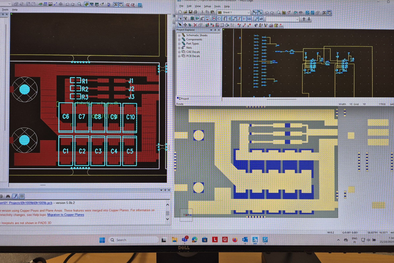
- Zuken CR-5000 and CR-8000
- PADS Professional
- Signal integrity and EMC analysis tools
These tools support rapid design iterations, thorough validation, and efficient transition from prototype to production.
Customer Outcome
Customer outcome
Sasken’s PCB engineering services help customers create reliable, manufacturable, and high-performance electronic products while reducing development risk.
Faster time-to-market through efficient design and validation
Improved signal integrity and system performance
Reduced development and manufacturing risks
Better EMC and thermal performance
Optimized cost and manufacturability
Seamless integration with RF, antenna, software, and mechanics
Long-term product reliability and lifecycle support
By combining PCB expertise with comprehensive product engineering capabilities, Sasken helps customers deliver products that perform reliably in real-world applications and demanding operating environments.

Have any Business Enquiries?
Got an idea you can't shake? Let's turn it into thriving business together.